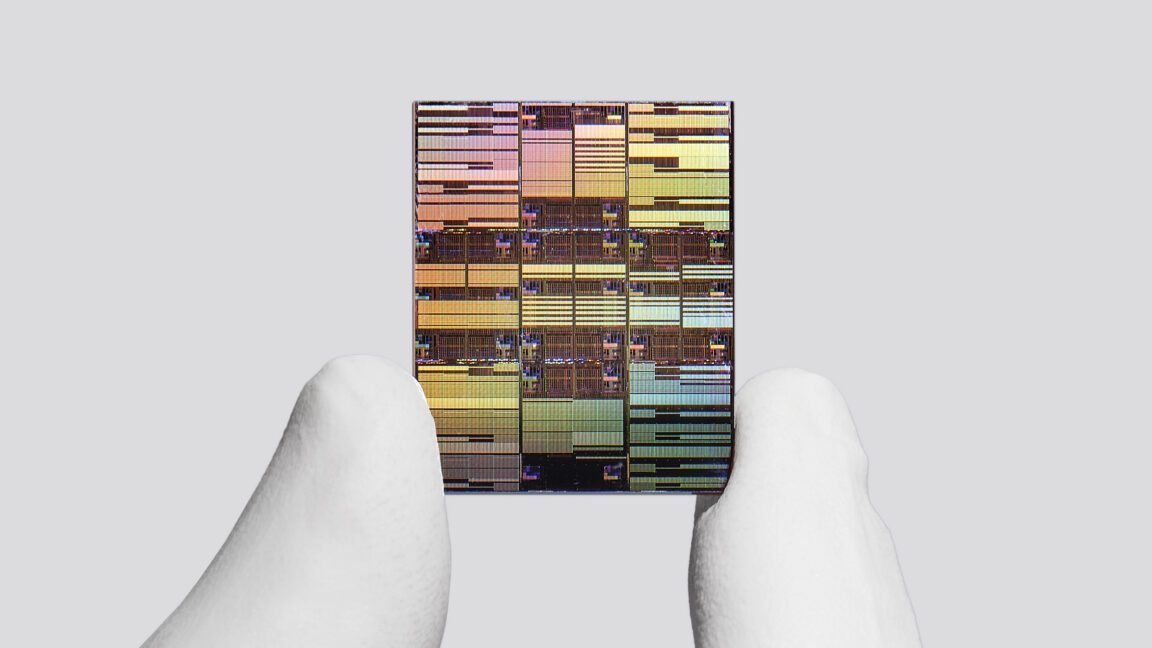
IBM has unveiled a new chip architecture that packs nearly 100 billion transistors into a tiny space, doubling the transistor density of its previous generation. This breakthrough, dubbed the ‘world’s first sub-1 nanometer chip technology’, promises significant improvements in computing performance and energy efficiency, particularly for AI data centers. The technology is expected to enable more powerful computing without a corresponding increase in energy consumption. Why it matters: this innovation could be a game-changer for the future of AI and computing, enabling faster and more efficient processing of complex data sets.
IBM's Tiny Chip
IBM has unveiled a new chip architecture that packs nearly 100 billion transistors into a tiny space, doubling the transistor density of its previous generation. This breakthrough, dubbed the 'world's first sub-1 nanomet…
Summarized from
Ars Technica AI AI-summarized
Was this helpful?
Discussion
Join the conversation
Comments are powered by GitHub Discussions. You need a GitHub account to participate.



The sharpest AI news, curated daily.
One email each morning. Summarized, sourced, and skimmable in under three minutes.
The sharpest AI news, curated daily.
One email each morning. Summarized, sourced, and skimmable in under three minutes.